
In the rapidly evolving world of semiconductor technology, the role of a Physical Design Engineer—often referred to as a Chip Physical Backend Engineer—is critical to transforming abstract circuit designs into manufacturable silicon chips. This position sits at the intersection of electrical engineering, computer science, and physics, requiring a unique blend of technical expertise and problem-solving skills. Below, we explore what this role entails, its significance in the chip development lifecycle, and the challenges these engineers face.

What Does a Physical Design Engineer Do?
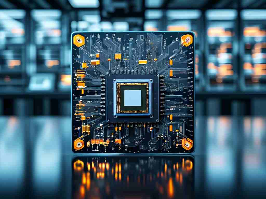
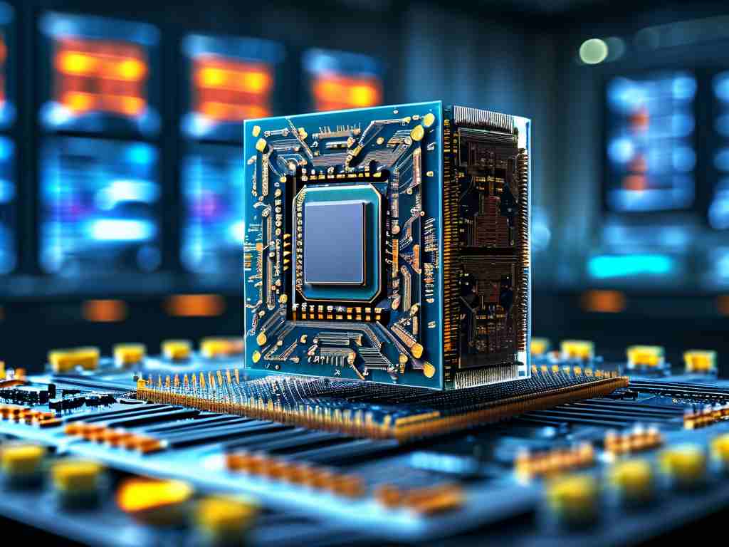
A Physical Design Engineer is responsible for the physical implementation of integrated circuits (ICs). This involves converting a high-level logical design—usually represented as a Register-Transfer Level (RTL) description—into a geometric layout that can be fabricated on silicon. Key tasks include:
-
Floorplanning:
Engineers partition the chip’s logical blocks into physical regions, considering power distribution, signal routing, and thermal management. This stage sets the foundation for subsequent steps and directly impacts performance and yield. -
Placement and Routing (P&R):
Transistors, gates, and other components are placed optimally on the silicon die. Engineers then route electrical connections between them while minimizing delays, power consumption, and signal interference. Tools like Cadence Innovus or Synopsys IC Compiler are often used here. -
Timing Closure:
Ensuring signals propagate correctly within clock cycles is paramount. Engineers analyze timing paths, adjust placements, and insert buffers to meet stringent timing constraints. -
Power Integrity and Signal Integrity Analysis:
With shrinking transistor sizes, power delivery networks must avoid voltage drops, and signals must be shielded from noise. Engineers simulate and refine designs to prevent reliability issues. -
Design Rule Checks (DRC) and Layout vs. Schematic (LVS):
Before tape-out (final submission to fabrication), the design undergoes rigorous verification to ensure compliance with foundry-specific manufacturing rules and consistency with the original schematic.
The Chip Development Workflow
Physical backend engineers operate within a multi-stage workflow:
- RTL to Gate-Level Netlist: The logical design is synthesized into a netlist of standard cells.
- Physical Implementation: Floorplanning, placement, routing, and optimization occur here.
- Verification: DRC, LVS, and electrical rule checks (ERC) validate manufacturability.
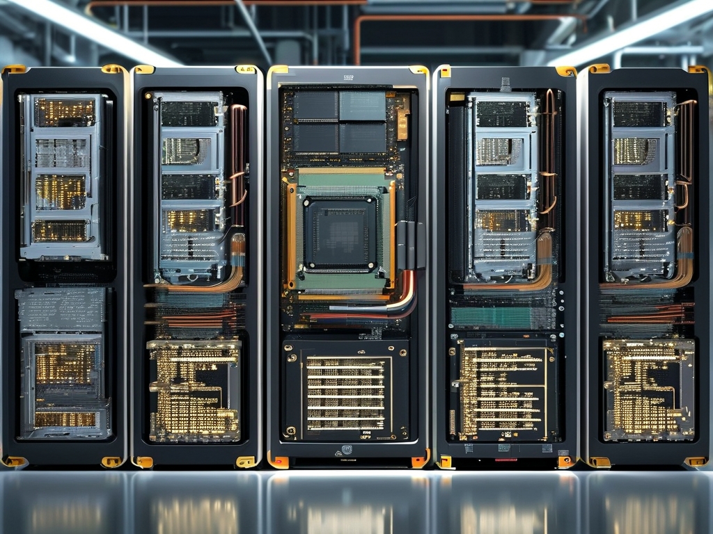
- Tape-Out: The finalized design is sent to a foundry (e.g., TSMC or Samsung) for fabrication.
Tools and Skills Required
Modern physical design relies heavily on Electronic Design Automation (EDA) tools. Engineers must master software like:
- Synopsys Fusion Compiler
- Cadence Innovus
- Siemens Calibre (for verification)
Technical skills include:
- Proficiency in scripting (Tcl, Python) for automation.
- Deep understanding of CMOS technology and semiconductor physics.
- Knowledge of advanced nodes (e.g., 7nm, 5nm) and their design challenges.
Soft skills like teamwork and communication are equally vital, as engineers collaborate with frontend designers, verification teams, and foundry partners.
Challenges in Physical Backend Design
-
Scaling Complexity:
As Moore’s Law pushes transistors to atomic scales, managing billions of components on a single die demands innovative routing algorithms and thermal solutions. -
Power and Heat Management:
High-performance chips generate significant heat. Engineers must balance performance with power efficiency, often using techniques like clock gating or dynamic voltage scaling. -
Manufacturing Variability:
At advanced nodes, microscopic imperfections during fabrication can affect yield. Engineers design redundancy and guardbands to mitigate these risks. -
Tight Timelines:
With market pressures to deliver chips faster, engineers must optimize workflows without compromising quality.
The Future of Physical Design Engineering
Emerging technologies like 3D-IC packaging and chiplets are redefining physical design. Engineers now work on stacking dies vertically and integrating heterogeneous components, requiring new tools and methodologies. Additionally, AI-driven EDA tools are automating repetitive tasks, allowing engineers to focus on high-level optimization.
Chip physical backend engineers are the unsung heroes of the semiconductor industry. Their work ensures that cutting-edge designs—from smartphones to AI accelerators—transition from abstract concepts to tangible, high-performance silicon. As technology advances, their role will only grow in complexity and importance, demanding continuous learning and adaptation.