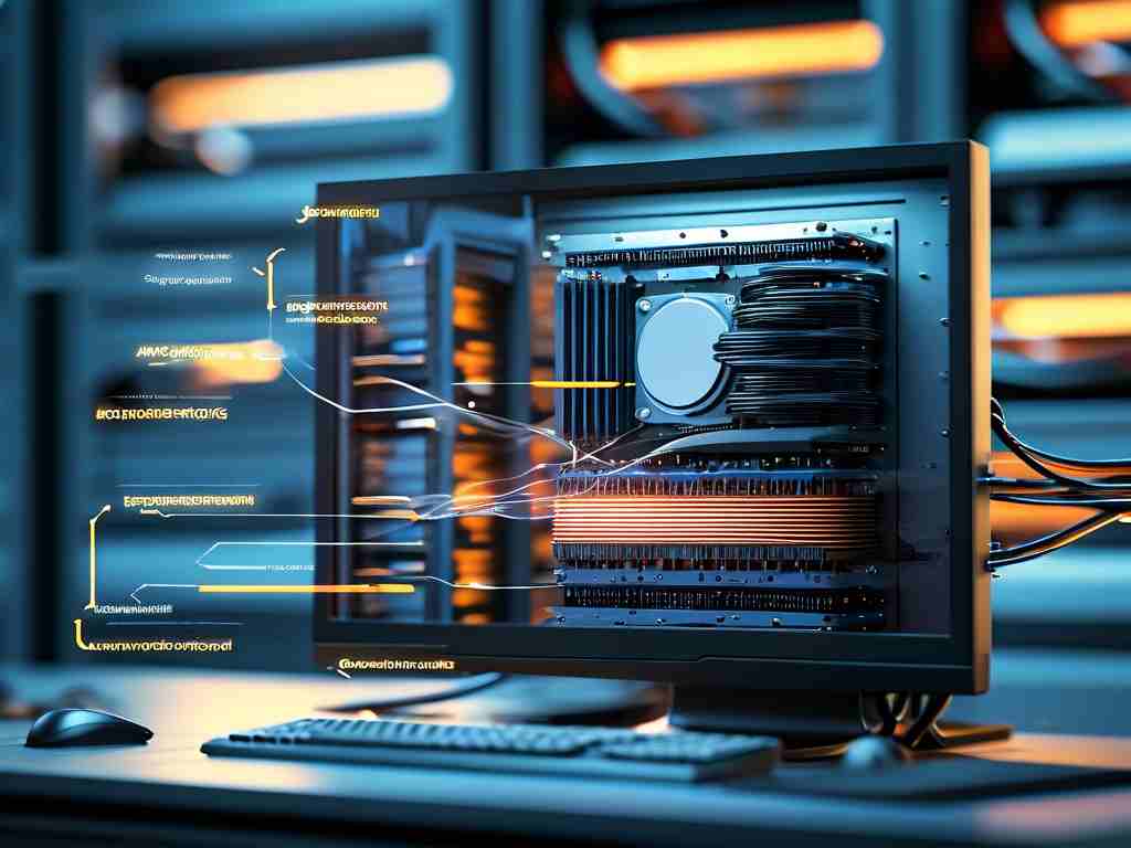

When you click a mouse or tap a keyboard, a complex chain of operations unfolds inside your computer to retrieve or modify data stored in memory. Understanding how computers access memory involves peeling back layers of hardware coordination and digital signaling. Let’s explore this intricate process while avoiding overly technical jargon.
At its core, memory access begins with a CPU request. When a program requires data, the central processing unit (CPU) generates a memory address through its memory management unit (MMU). This address points to a specific location in the physical or virtual memory space. Modern systems often use virtual addressing, where the MMU translates logical addresses into physical ones using page tables. This layer of abstraction allows programs to operate as if they have exclusive access to memory while the OS manages actual resource allocation.
Next, the request travels via the memory bus, a communication channel connecting the CPU to RAM. The bus consists of three components: an address bus to specify locations, a data bus to transfer information, and a control bus to manage timing signals. For example, when reading data, the CPU sends a "read" command through the control bus alongside the target address. The memory controller—a dedicated chip on the motherboard or integrated into modern CPUs—orchestrates this exchange.
Once the memory controller receives the request, it activates the appropriate DRAM module. Dynamic RAM (DRAM) stores data in capacitors that must be refreshed thousands of times per second. To retrieve information, the controller sends row and column addresses to open a specific "cell" in the memory matrix. This process, called row activation, copies an entire row of data into a buffer. The controller then selects the exact column to extract the required bits.
During a write operation, the CPU follows a similar path but sends data instead of a read signal. The memory controller updates the target cell’s charge state to represent new binary values. However, DRAM’s design introduces latency. For instance, after accessing a row, the controller must wait for a precharge phase to reset the row before accessing another. This delay, measured in nanoseconds, impacts overall system performance.
Caching plays a critical role in optimizing memory access. Modern CPUs include L1, L2, and L3 caches—small, ultra-fast memory pools that store frequently used data. When the CPU requests information, it first checks these caches. If the data is present (a cache hit), it’s retrieved in 1-3 clock cycles, vastly quicker than accessing RAM. Cache misses, however, force the CPU to wait for slower main memory.
Let’s examine a real-world analogy. Imagine a librarian (CPU) searching for a book (data). Instead of visiting the entire library (RAM) every time, they keep popular titles on a nearby cart (cache). Only when a requested book isn’t on the cart does the librarian walk through the shelves. Prefetching algorithms further enhance this by predicting which books might be needed next and placing them on the cart in advance.
Error correction is another silent guardian in memory operations. Technologies like ECC (Error-Correcting Code) memory detect and fix single-bit errors using parity checks. When writing data, ECC RAM generates checksums. During reads, it recalculates these values and corrects discrepancies caused by cosmic rays or electrical interference—a vital feature for servers and critical systems.
In multi-core processors, memory access becomes a dance of coordination. Cores share access to RAM through protocols like MESI (Modified, Exclusive, Shared, Invalid), which maintain cache coherence across cores. If one core modifies data cached by another, the protocol ensures all copies stay synchronized, preventing conflicts.
Finally, the retrieved data returns to the CPU via the data bus. The entire process—from initial request to data delivery—might take 50-100 nanoseconds for DRAM but just nanoseconds for cache access. While seemingly instantaneous, these microseconds compound in performance-critical applications like gaming or scientific computing, driving innovations in memory technology such as DDR5 and HBM (High Bandwidth Memory).
In summary, computer memory access is a symphony of hardware components and protocols working in tandem. From address translation to error checking, each step ensures data flows efficiently between processors and storage. As software demands grow, understanding these mechanisms becomes crucial for optimizing performance and advancing computational capabilities.