
Soldering is a critical skill for developers working with embedded systems, particularly when prototyping or modifying custom development boards. While automated assembly dominates industrial production, hands-on soldering remains essential for debugging, component replacement, and small-batch projects. This guide explores professional techniques and best practices for achieving reliable solder joints on embedded hardware.
Understanding Thermal Dynamics
Embedded boards often contain heat-sensitive components like microcontrollers and sensors. Use a temperature-controlled soldering iron set between 300°C (572°F) and 350°C (662°F) for lead-free solder. For QFN or BGA packages, consider preheating the PCB to 100°C–150°C using a hot air station to prevent thermal shock. A common mistake is applying heat for too long – the golden rule is to complete each joint within 3 seconds.
Tool Selection Matters
Invest in a precision soldering iron with interchangeable tips. A chisel tip (1.6mm–2.4mm) works best for through-hole components, while a conical tip (0.5mm–1mm) handles surface-mount devices (SMDs). Keep brass wool for tip cleaning instead of traditional sponges, as they maintain consistent tip temperature. For desoldering, pair a quality vacuum pump with high-temperature braided copper wick.
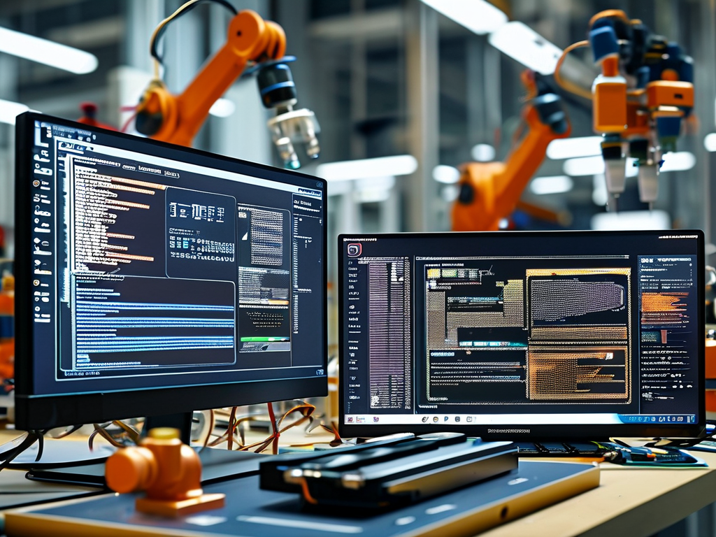
Code-Driven Soldering Validation
Incorporate automated testing after manual soldering. For example, use OpenOCD to verify electrical connections through boundary scan:
openocd -f interface/stlink-v2.cfg -f target/stm32f4x.cfg
> init
> scan_chain
This checks for open circuits in JTAG/SWD interfaces. For power delivery validation, write a quick Python script using pySerial to monitor voltage rails:
import serial
ser = serial.Serial('/dev/ttyUSB0', 115200)
while True:
    print(ser.readline().decode().strip())
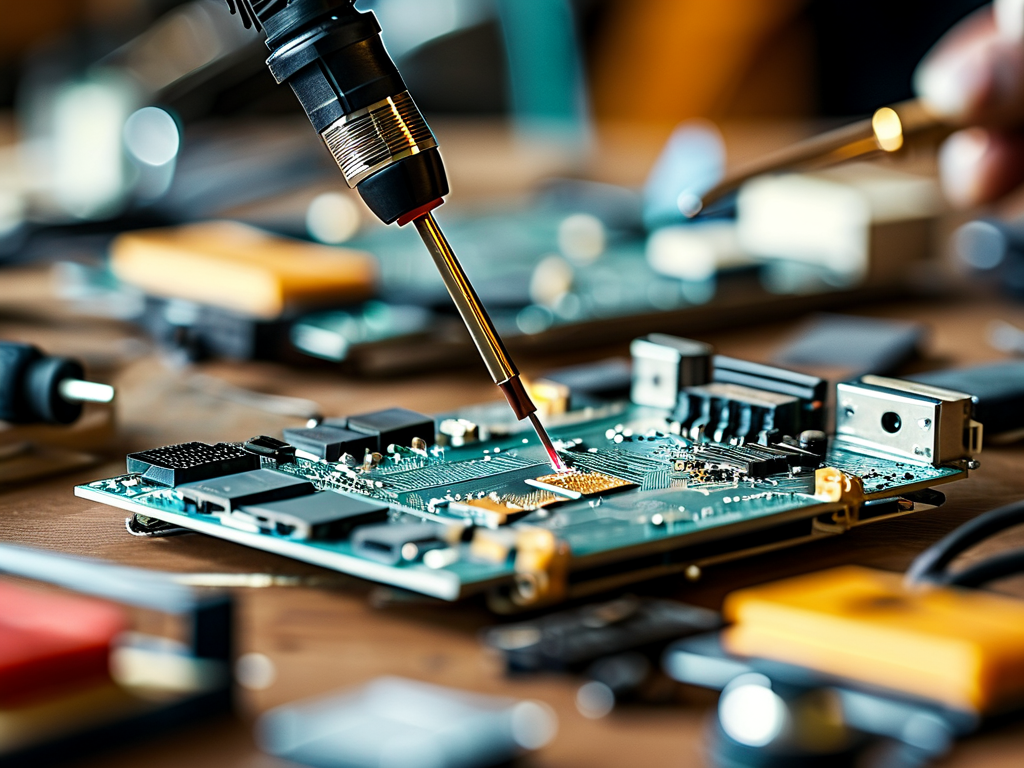
SMD Handling Techniques
When working with 0402 or smaller packages, apply flux paste before positioning components. Use reverse-action tweezers for stable placement. For ICs with hidden pins (e.g., QFN), drag soldering with a beveled tip creates reliable connections. After soldering, inspect joints under 10x magnification – proper joints should exhibit concave fillets with visible lead outlines.
Troubleshooting Common Issues
Cold joints (dull, grainy appearance) indicate insufficient heat – reflow with added flux. Bridged pins require desoldering braid and flux reapplication. If a pad lifts due to overheating, repair using conductive epoxy and a micro-copper patch. For stubborn components, apply low-melt solder (e.g., Chip Quik SMD291) to reduce removal temperature.
ESD Protection Protocols
Always use a grounded workstation and wrist strap when handling embedded components. Store sensitive ICs in anti-static foam, and never place bare PCBs directly on synthetic surfaces. For added protection, implement ESD-safe soldering iron tips and grounded mats.
Advanced Rework Strategies
When upgrading firmware interfaces, consider adding test points during initial soldering:
// Add debug headers in code
#define DEBUG_ENABLE 1
#if DEBUG_ENABLE
    #define DEBUG_PIN GPIO_PIN_12
    void debug_init() {
        __HAL_RCC_GPIOB_CLK_ENABLE();
        GPIO_InitStruct.Pin = DEBUG_PIN;
        GPIO_InitStruct.Mode = GPIO_MODE_OUTPUT_PP;
        HAL_GPIO_Init(GPIOB, &GPIO_InitStruct);
    }
#endif
This allows easier signal probing without disturbing existing solder joints.
Material Science Considerations
Select solder alloys based on application requirements:
- SAC305 (96.5% Sn, 3% Ag, 0.5% Cu): General-purpose, high-reliability
- SN100C (99.3% Sn, 0.7% Cu, Ni+Ge): Reduced whiskering risk
- Indium-based alloys: Cryogenic or high-vibration environments
Pair with no-clean flux to minimize post-assembly residue. For high-density interconnects, use solder paste with Type 4 powder (20–38μm particle size).
Future Trends
The rise of 0.4mm-pitch BGA packages and embedded wafer-level packages (eWLP) is pushing manual soldering to its limits. Developers are adopting hybrid approaches – using hot plates for global heating while performing local rework with micro-irons. New conductive adhesives that cure at 150°C may eventually supplement traditional soldering for temperature-sensitive MEMS devices.
Mastering these techniques requires practice but significantly improves prototyping efficiency and hardware reliability. Always document soldering parameters (iron temperature, dwell time, alloy type) for process repeatability. As embedded systems grow more complex, precise soldering remains a fundamental skill bridging digital designs with physical implementations.