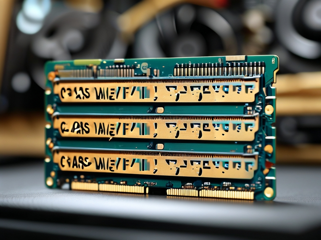
Memory timing parameters play a critical role in determining the performance and stability of computer systems, particularly for tasks requiring high-speed data processing like gaming, video editing, and scientific computing. This guide will explain how to calculate memory timing parameters, their significance, and practical steps to optimize them.

1. What Are Memory Timing Parameters?
Memory timing refers to the latency intervals between operations in a RAM module. These parameters are expressed as a series of numbers (e.g., 16-18-18-36) and are measured in clock cycles. The four primary timing parameters are:
- CAS Latency (CL): The delay between a memory controller requesting data and the RAM module responding.
- tRCD (RAS to CAS Delay): The time required to activate a row (RAS) and access a column (CAS).
- tRP (Row Precharge Time): The delay to close one row and open another.
- tRAS (Row Active Time): The minimum time a row must remain open for reliable data access.
2. Why Calculate Memory Timing Parameters?
Optimizing these timings improves system responsiveness and reduces bottlenecks. Tightening timings (lower values) can boost performance, but overly aggressive settings may cause instability. Calculating these values ensures a balance between speed and reliability.
3. Key Formulas and Variables
To calculate memory timing parameters, you need:
- Memory Clock Speed (MHz): The operating frequency of the RAM.
- CAS Latency (CL): Determined by the memory module's specifications.
- Nanoseconds per Cycle: Calculated as ( \frac{1000}{\text{Clock Speed (MHz)}} ).
Example Calculation: For DDR4-3200 RAM (1600 MHz base clock) with CL16: [ \text{Latency (ns)} = \frac{CL \times 2000}{\text{Clock Speed}} = \frac{16 \times 2000}{3200} = 10 \text{ ns} ]
4. Steps to Calculate and Adjust Timings
Step 1: Identify Default Timings Check your RAM's stock timings using tools like CPU-Z, Thaiphoon Burner, or BIOS/UEFI settings.
Step 2: Calculate Theoretical Limits Use the formula above to convert clock cycles to nanoseconds. Compare these values with manufacturer-recommended specifications to avoid instability.
Step 3: Test Incremental Adjustments Gradually lower timing values (e.g., reduce CL from 16 to 15) and stress-test the system using MemTest86 or Prime95. Monitor for errors or crashes.
Step 4: Account for Voltage and Temperature Lower timings may require increased DRAM voltage (e.g., 1.35V to 1.4V). Ensure proper cooling to prevent overheating.
Step 5: Secondary and Tertiary Timings Advanced users can adjust subtimings like tRFC (Refresh Cycle Time) or tWR (Write Recovery Time) for finer optimization.
5. Tools for Timing Management
- Ryzen DRAM Calculator: For AMD systems, this tool suggests optimal timings based on RAM type.
- Intel XMP Profiles: Pre-configured overclocking profiles for Intel platforms.
- BIOS/UEFI Interface: Directly modify timings and voltages for granular control.
6. Common Pitfalls and Solutions
- Over-tightening Timings: Causes system crashes. Revert to stable values and test incrementally.
- Incompatible Hardware: Ensure the motherboard supports the desired RAM speed and timings.
- Voltage Limitations: Exceeding safe voltage thresholds (e.g., >1.5V for DDR4) risks damaging components.
7. Real-World Performance Impact
In benchmarks, optimized timings can improve frame rates in games by 5–10% and reduce rendering times in applications like Blender. However, gains diminish beyond a point, emphasizing the need for balanced tuning.
8.
Calculating memory timing parameters requires a mix of technical knowledge and systematic testing. By understanding the relationships between clock speed, latency, and voltage, users can unlock hidden performance while maintaining system stability. Always prioritize incremental changes and validate results with stress tests.


